


Comprehensive Strategic Evolution of Non-Volatile Memristive Switching, In-Memory Computing, and Neuromorphic Synaptic Architectures
Modern artificial intelligence compute accelerators, low-power edge neural inferencing nodes, ultra-dense non-volatile storage-class memories, and bio-inspired neuromorphic computing platforms depend fundamentally on non-von Neumann computing architectures, establishing the operational foundation of the Memristor Industry. For over seven decades, digital computing architectures adhered to the classical von Neumann model: physically separating the central processing unit (CPU) from memory storage (DRAM/NAND flash). As deep neural networks scaled to hundreds of billions of synaptic weight parameters, shuttling data back and forth across physical interconnect buses created the "von Neumann Memory Wall"—an architectural bottleneck that accounts for over sixty to eighty percent of total computational energy dissipation and introduces microsecond latency delays. Memristors—the fourth fundamental passive circuit element conceptualized by Leon Chua in 1971 and experimentally realized in thin-film titanium dioxide by HP Labs in 2008—resolve these structural processing bottlenecks. By altering their internal electrical resistance (M=dϕdqM = \frac{d\phi}{dq}M=dqdϕ) in response to the history of applied electrical voltage and retaining that non-volatile conductive state without external power, memristors combine high-density non-volatile memory storage with in-situ analog arithmetic computation directly on a single nanoscale device.
The foundational engineering of contemporary memristive devices centers on nanoscale transition metal oxide switching, conductive filamentary ionics, and crossbar array cross-point scaling. In a typical Valence Change Memory (VCM) memristive device, a thin transition metal oxide dielectric switching layer—such as titanium dioxide (TiO2TiO_2TiO2), hafnium oxide (HfO2HfO_2HfO2), or tantalum oxide (Ta2O5Ta_2O_5Ta2O5) measuring between 3 and 10 nanometers in thickness—is sandwiched between an inert top electrode (platinum or titanium nitride) and a reactive bottom electrode. When an electrical programming voltage pulse is applied, electric fields exceed megavolts per centimeter, causing negatively charged oxygen ions (O2−O^{2-}O2−) to drift toward the reactive electrode, leaving behind localized nanoscale filaments of positively charged oxygen vacancies (VO∙∙V_O^{\bullet\bullet}VO∙∙). These conductive vacancy filaments bridge the two electrodes, transitioning the device from a high-resistance state (HRS) to a low-resistance state (LRS). Applying a reverse polarity electric field pushes oxygen vacancies back, re-oxidizing the conductive filament and returning the device to HRS. In Electrochemical Metallization (ECM) or conductive-bridging RAM (CBRAM) devices, mobile metal cations (silver or copper) drift through a solid electrolyte dielectric matrix (such as chalcogenide glass or silicon oxide) to form metallic atomic bridge filaments. Modern memristors deploy Crossbar Array (1T1R or 1S1R) architectures: integrating a threshold vacuum selector (1S) or access transistor (1T) at every perpendicular wire intersection to eliminate "sneak-path" parasitic leakage currents across adjacent cells, enabling sub-20nm cell scaling and 3D multi-layer vertical monolithic stacking.
Deploying comprehensive memristor platforms delivers decisive computational throughput, energy efficiency, and storage-class latency advantages across artificial intelligence hardware and spaceborne computing. In In-Memory Computing (IMC) and Neuromorphic Processing, memristor crossbar arrays execute Analog Vector-Matrix Multiplication (VMM)—the mathematical core of deep neural network forward-pass inference—in a single computational step: by applying input voltage vectors across crossbar rows, each memristive cell modulates current proportional to its conductance under Ohm’s Law (I=V⋅GI = V \cdot GI=V⋅G), and column bitlines sum the currents natively under Kirchhoff’s Current Law (Iout=∑Vi⋅GijI_{\text{out}} = \sum V_i \cdot G_{ij}Iout=∑Vi⋅Gij). Executing analog matrix math directly within the physical memory cells eliminates the von Neumann bus transfer entirely, achieving energy efficiencies exceeding tens to hundreds of Tera-Operations Per Second per Watt (TOPS/W). In high-density non-volatile storage, memristors provide read and write latencies in the single-digit nanosecond range—operating hundreds of times faster than traditional 3D NAND flash while approaching DRAM switching speeds—with multi-level cell (MLC) capabilities storing multiple analog bits per nanoscale cell. Furthermore, in radiation-hardened defense and space computing, oxide-based memristive filaments are immune to cosmic ray single-event upsets (SEU) and total ionizing dose (TID) radiation that destroy conventional floating-gate charge-storage transistors.
Looking toward strategic long-term microelectronics roadmaps, memristive architectures are converging with bio-mimetic synaptic plasticity, 3D vertical resistive RAM (3D-VRRAM), and atomic-scale neuromorphic spiking neural networks (SNNs). Advanced memristors demonstrate dynamic Spike-Timing-Dependent Plasticity (STDP)—a biological learning rule where the synaptic conductance weight changes gradually based on the relative timing delays between incoming pre-synaptic and post-synaptic action potential spikes—enabling autonomous, unsupervised edge machine learning on battery-free hardware. Concurrently, semiconductor foundries are integrating memristor back-end-of-line (BEOL) thin films between the metal interconnect layers of standard 300mm CMOS silicon wafers at temperatures below 400°C, stacking dense memory arrays directly atop digital CMOS arithmetic logic without degrading front-end silicon transistors. Supported by open hardware consortia and international JEDEC non-volatile memory standardization bodies, memristors maintain an indispensable foundation driving the post-Moore's Law semiconductor transition toward brain-inspired computing, ultra-dense non-volatile storage, and edge intelligence worldwide.
Top Trending Reports :
Machine Learning Consulting Services Market
Marketing And Branding Consulting Services Market
Marketing Data Analytics Services Market
Mechanical Engineering Consulting Services Market
Mediation And Arbitration Services Market
Categorias
Leia Mais
Market Overview Surgical patient safety continues to advance as hospitals adopt technology-driven solutions to eliminate preventable surgical errors. The Sponge Counting System Market is projected to grow through 2030, driven by rising surgical procedure volumes, growing regulatory emphasis on patient safety protocols, and increasing hospital investment in radiofrequency and barcode-based...

Fluid power equipment transmits force through pressurised liquids and gases, underpinning earthmoving machinery, factory automation and agricultural equipment. According to Market Research Future, hydraulic transmission systems account for 64.8% of the market's revenue, sustaining their position through unmatched power density in construction and drilling applications. The overall market was...
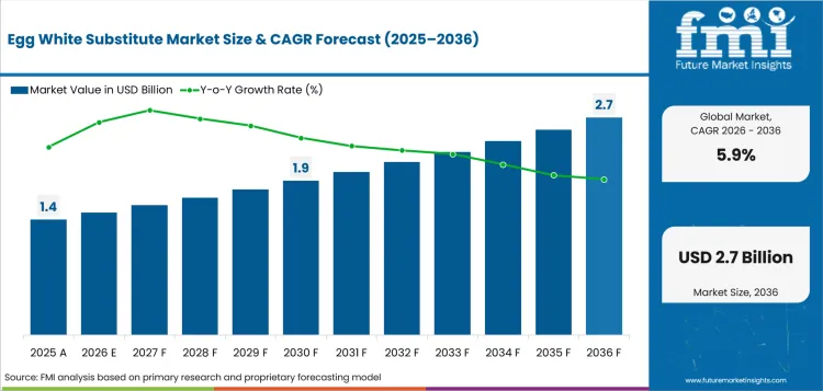
NEWARK, Del., October 14, 2026 — The global Egg White Substitute Market gaining traction as commercial bakeries and food manufacturers seek reliable alternatives to conventional egg whites amid price volatility, supply disruptions, and growing demand for plant-based food formulations. According to the latest market intelligence report published by Future Market Insights (FMI), the market...
Digital transformation is rapidly reaching laboratory containment infrastructure through IoT integration and centralized facility monitoring platforms. Smart safety cabinets now incorporate wireless telemetry, automated sensor calibration, and continuous cloud-based logging of airflow velocities and filter conditions. To explore digital equipment integration models, sensor technology...
The Immobilized Trypsin Treated With TPCK Market is witnessing significant growth as biotechnology and pharmaceutical industries increasingly rely on high-performance enzymes for protein analysis, drug development, and diagnostic applications. Immobilized trypsin treated with TPCK (N-Tosyl-L-phenylalanyl chloromethyl ketone) is a specialized enzyme preparation that offers enhanced stability,...