

High-Bandwidth Memory Stacking and Optical Interconnect Technologies Reshaping Modern Compute Topologies
Modern high-performance computing hardware and enterprise server clusters are undergoing an architectural evolution, moving away from conventional motherboard bus layouts toward dense, integrated computing topologies that leverage the latest data center accelerator market trends to eliminate memory access bottlenecks, reduce signal latency, and expand computing bandwidth. Hardware architects face a major challenge known as the "memory wall": while accelerator compute core performance has scaled rapidly, traditional external DDR memory buses cannot supply data fast enough to keep thousands of arithmetic units fully saturated. When compute cores sit idle waiting for memory retrieval, total system throughput drops and electrical power is wasted. Modern accelerator architectures overcome this limitation by combining 3D-stacked High-Bandwidth Memory (HBM), advanced silicon interposers, and co-packaged optical interconnects, creating integrated computing packages that deliver massive data bandwidth with low latency.
A defining technological development in the sector is the integration of High-Bandwidth Memory (such as HBM3e and emerging HBM4) directly adjacent to the main accelerator processing die. In an HBM architecture, multiple dynamic RAM (DRAM) dies are stacked vertically using thousands of micro-machined Through-Silicon Vias (TSVs) and bonded to a passive silicon interposer. This 3D stacking structure provides a wide 1024-bit memory interface per stack—compared to narrow 32-bit or 64-bit interfaces on traditional DDR memory modules—delivering memory bandwidths exceeding one terabyte per second per stack. By placing four to eight HBM stacks around a central compute processor, modern AI accelerators achieve aggregate memory bandwidths of several terabytes per second, allowing massive neural network weights to be read and updated in real time without processing stalls.
+-----------------------------------------------------------------------------------------+
|                  ADVANCED DATA CENTER ACCELERATOR SILICON STACK PROFILE                 |
+---------------------+-------------------------------------------------------------------+
| COMPUTE TIER        | Deep Sub-Micron Logic Die (3nm/2nm) | Dedicated Tensor Math Cores |
+---------------------+-------------------------------------------------------------------+
| MEMORY TIER (3D)    | Multi-Layer High-Bandwidth Memory (HBM3e/HBM4) via Vertical TSVs  |
+---------------------+-------------------------------------------------------------------+
| INTERPOSER LAYER    | High-Density Silicon Interposer (2.5D) | Fine-Pitch Micro-Bumps   |
+---------------------+-------------------------------------------------------------------+
| OPTICAL I/O TIER    | Co-Packaged Optics (CPO) Engine | Multi-Channel Silicon Photonics |
+---------------------+-------------------------------------------------------------------+
| SUBSTRATE & THERMAL | High-Density Organic Substrate | Integrated Liquid-Cooled Cold Pl.|
+-----------------------------------------------------------------------------------------+
Another major operational trend is the transition from electrical copper traces to Co-Packaged Optics (CPO) and silicon photonics for inter-server communications. As data rates climb toward 800 Gbps and 1.6 Tbps per network port, transmitting high-frequency electrical signals over conventional copper backplanes and Twinax cables causes severe signal attenuation, heat dissipation, and electromagnetic interference. Co-packaged optics solves this issue by integrating optical transceiver engines directly onto the same substrate as the compute accelerator die. Electrical signals are converted into optical laser pulses within millimeters of the processing cores, allowing high-bandwidth data to travel across optical fibers directly to neighboring server racks without bulky external transceiver modules or energy-intensive retimer chips, slashing networking power consumption by up to thirty percent.
Unified software abstraction layers and automated compilation toolchains represent an additional technological milestone for the data center accelerator ecosystem. Historically, programming different types of accelerators required specialized, fragmented software environments—such as CUDA for GPUs, OpenCL for heterogeneous devices, and hardware description languages (VHDL/Verilog) for FPGAs. Modern software stacks provide cross-platform abstraction frameworks that compile high-level neural network code (such as PyTorch and TensorFlow) across diverse GPU, ASIC, and DPU hardware platforms automatically. These intelligent compilers optimize mathematical graph execution, partition tensor layers across distributed accelerator clusters, and manage memory caching automatically. By combining high-bandwidth 3D memory stacking, co-packaged optical networking, and unified software compilers, modern data center acceleration platforms deliver the processing speed and efficiency required for contemporary computing workloads.
Top Trending Reports :
Us Digital Signal Processors (Dsp) Market
Categorie
Leggi tutto
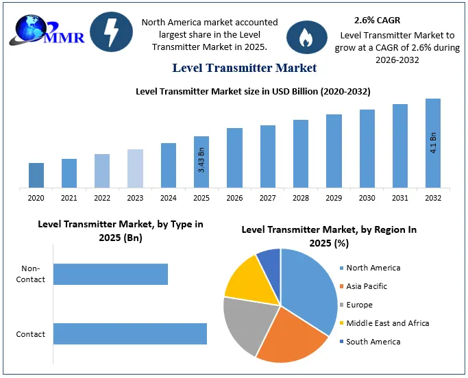
Market Overview The Level Transmitter Market is witnessing steady expansion as industries increasingly adopt automated, accurate, and continuous measurement technologies for monitoring liquids, slurries, powders, and bulk solids. According to the latest report by Maximize Market Research (MMR), the global Level Transmitter Market was valued at approximately USD 3.43 billion in 2025...
Market Overview The immobilized enzyme reactor market is expanding as biocatalytic processing gains preference across pharmaceutical, food, and industrial chemical production. The market is projected to grow through the coming years, driven by rising demand for sustainable manufacturing processes, growing pharmaceutical biocatalysis applications, and continuous advancement in enzyme...

Market OverviewEnvironmental safety is becoming an increasingly critical concern in Italy, significantly influencing the solid phase extraction market. As regulations surrounding environmental protection tighten, industries are required to adopt sustainable practices and reliable analytical methods for monitoring contaminants. Solid phase extraction offers a more environmentally friendly...
The report titled ‘ADC Contract Manufacturing Market(7th Edition) Forecast 2026 to 2035’ delivers a structured overview of how the industry has progressed over the years, along with expectations for future movement till 2035. This report evaluates changes in the market size and highlights important developments within the industry. It offers clarity on regional patterns, key...

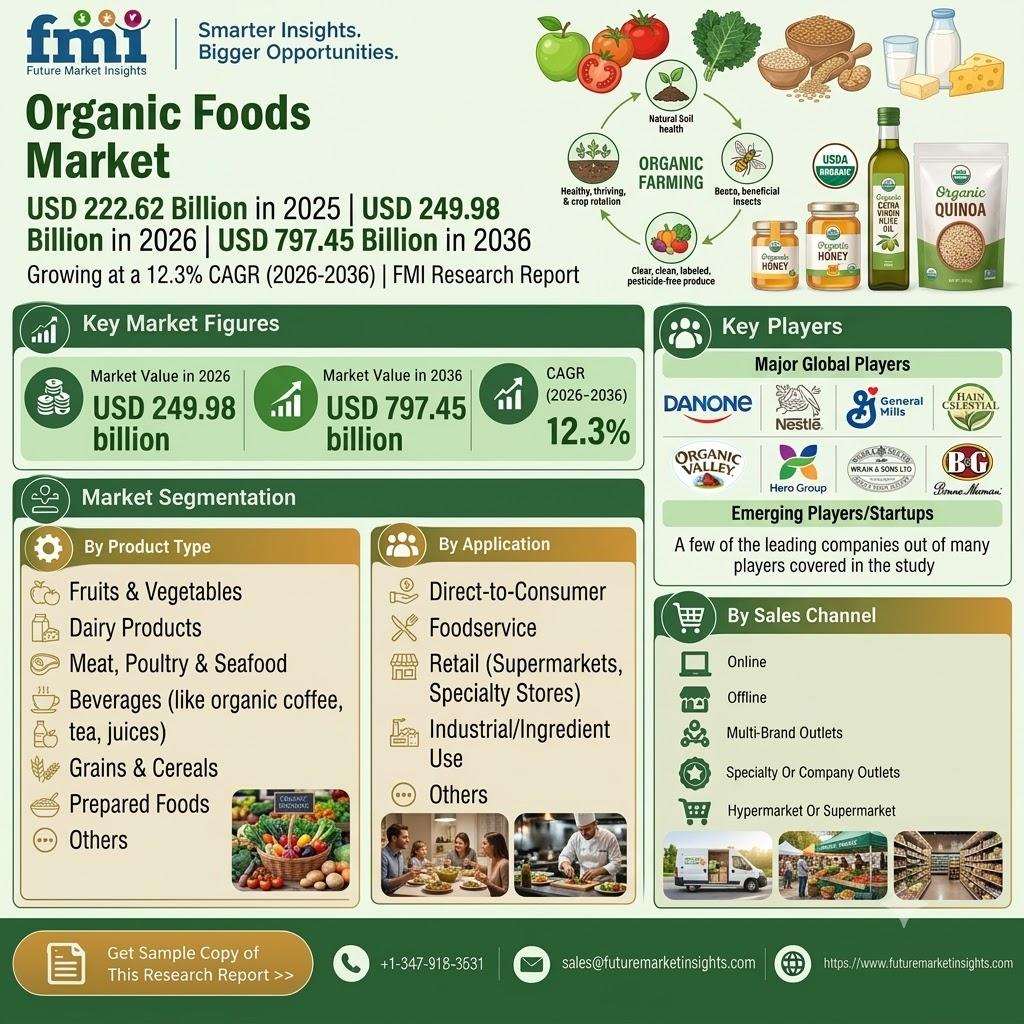
Organic Foods Market By FMI Syndicated, Customized FMI Report News NEWARK, Del., October 13, 2026. — The global Organic Foods Market was valued at USD 222.62 billion in 2025 and is projected to reach USD 249.98 billion in 2026, expanding to USD 797.45 billion by 2036 at a CAGR of 12.3% from 2026 to 2036, according to Future Market Insights (FMI). The growth outlook is being shaped by...